Clock Monitors in SoC Verification
August 6, 2021 2022-02-01 18:32Clock Monitors in SoC Verification

Clock Monitors in SoC Verification
Introduction
As technologies advance, we see increasingly complex SoCs in the market, SoCs that have various wireless modules, and processors that use new bus architectures to communicate with them. They can also have various interfaces like I2C, PCM, I2S, AHB, etc. Yet, these SoC components will share a single clock control unit. This module generates the various clock inputs for IPs and protocols, enabling them to function seamlessly.
Each module may require a different clock frequency based on the divider settings, which can be programmed through registers. Often, some IPs and protocols will require changes to the clock frequency on the fly. For verification, one should test all possible combinations of clock frequencies that their control unit supports, and check that the modules operate without a glitch. This can easily be verified by what is called a clock monitor. This paper presents the concept of a reusable clock monitor that can verify complex clock systems.
The semiconductor industry is in a constant race to be first-to-market with a significant first-mover advantage. This puts pressure on the verification process, to shrink overall development time. In SoCs, the clock control unit is critical, and this is not a standard IP.
A clock monitor is a SV/UVM based component to monitor the clock under test. As the functionality of the clock monitor is unique and flexible, and can we re-use it on different types of SoCs.
These are the functions of a clock monitor
- Check the clock frequency with user specified tolerance
- Detect glitches (including the zero time glitch)
- Check on-the-fly frequency switching functionality
- Generate alerts in case of timeouts
- Enable/disable clock monitor in run time
- Measure duty-cycle with user specified tolerance
- Check the DC value of clock when clock is stopped
- Cover the frequency being measured
Diagram represents the block diagram of the clock monitor component. Clock monitor clk_mon_c is extended from the uvm_monitor so that it has the features of uvm_monitor. This monitor is encapsulated in a uvm_agent – clk_mon_agent_c.
The clock has a virtual interface connected to it – clk_mon_if. This virtual interface has only two signals: clk and enable. clk signal of clk_mon_if should be connected to the SoC clock to connectivity to the clock enable signal of the SoC. This uvm_agent can be instantiated inside any uvm_env.
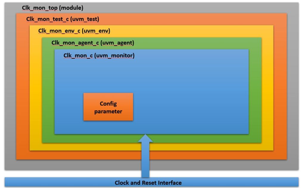
This clock monitor has certain configuration parameters which are user-programmable. This can be passed to the clock monitor from the UVM environment or a test case through the set_config_db and get_config_db method of UVM.
Here is the list of such configuration parameters.
- bit Enable/disable : Enable or Disable the clock monitor (on the fly)
- real Input frequency : Frequency at which clock is running (MHz)
- real Freq tolerance : Specify the frequency tolerance (percentage)
- real High Period : Specify the High Period of Clock (Percentage)
- real Low Period : Specify the Low Period of Clock (Percentage)
- real Switch Freq : Frequency at which Clock should be switched (MHz)
- real Switch_high Period : High Period of Clock for the switched clock (Percentage)
- real Swtich_low Period : Low Period of Clock for the switched clock (Percentage)
- bit switch enable : Inform Clock Monitor that switching of the frequency is expected
- real freq_all [] : Dynamic array of possible frequencies for a given clock (MHz)
- bit freq_expected : When set, it indicates that the frequency in operation should be within the frequency specified by freq_all array, when reset disables this checking
- bit dc value : Clock dc value at reset time
- int switch_freq_tolerance : Indicates how many clock cycles can be ignored while switching is in place (Default is one)
Advantages of clock monitors
- Reusable Module, saves time and effort
- Measures accurate Clock on every clock cycle, reduced possibility of human error
- Automatically detects the Glitch including the zero time glitch on Clock
- Wide frequency measurement range, not limited by equipment
- Detects switching of clock frequency
- Automates checking, generates custom alerts
- Measures duty-cycle of the clock
In general, using a clock monitor saves time and effort in verifying the SOC clock and control block. As the clock monitor presented in this doc is fully reusable, we can plug and play this on any SoC or IP. It can also measure the frequency it has covered with the help of the coverage component.
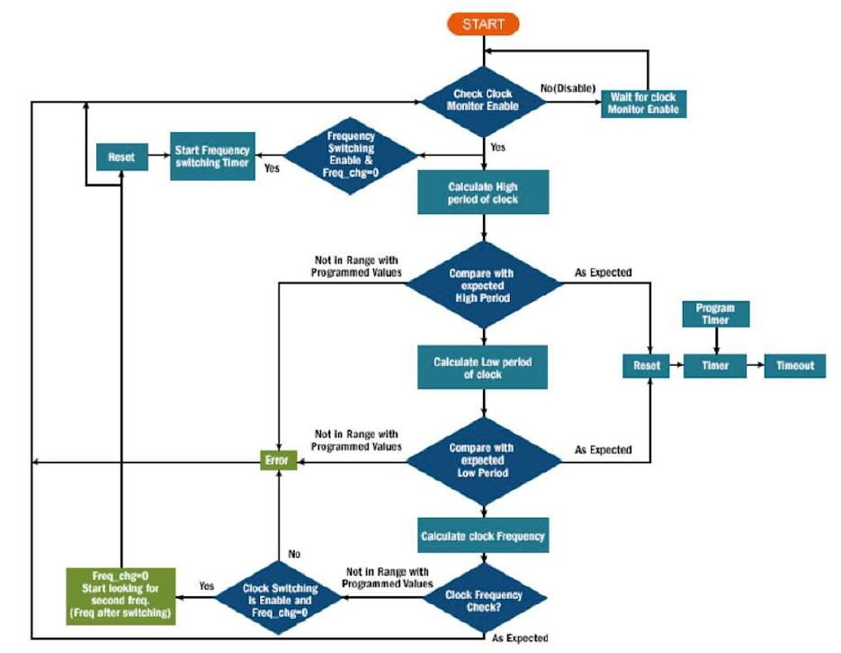
Flow chart
Diagram shows the flowchart of the clock monitor. Once the enable signal is set for the clock monitor it will start monitoring. Now, the clock monitor captures the high and low periods of the clock from the posedge and negedge. If the calculated high and low periods are not within the expected tolerance, it will alert a uvm_error. If neither posedge nor negedge is observed within the specified timeout period, the Clock Monitor will generate a uvm_error for the timeout. For clock switching, first, the clock monitor will check if a clock switch is expected or not. If not, then it would generate a uvm_error. If switching is expected, then after the first few clock cycles post switching (based on the parameter set by user), we start checking the new High and Low Periods (frequency) versus the expected values. If they are not within the expected tolerance range, then the Clock Monitor will generate a uvm_error. If at any time, the measured frequency is not within the array of the specified range, a uvm_error will be reported.
If frequency switching is expected and it does not take place, then a timeout error would be reported.
Example
We used the clock monitor to verify an SoC, with multiple wireless IPs like Bluetooth, GPS, FM, and serial protocols like UART, IIC, and SPI. Each IP and protocol operated at a different frequency, and would also switch clocks during low power mode (on the fly). Using the clock monitor in this project saved time in verifying the clock frequency compared with some of the traditional approaches of directed testing.
The coverage component of the clock monitor adds an extra advantage that any frequency measured by the clock monitor is not covered. So instead of using the directed tests for the clock, now system Verilog random constraint-driven test cases can be used to verify the clocks which again saves time, and requires less maintenance. Having already developed this clock monitor in System Verilog (UVM based), now this is reusable in any other SoC or IP project where clock verification is needed. So for the new projects, this saves more time as no development is needed you can simply plug the clock monitor in your existing System Verilog UVM based environment and start verification of clock block from day one.
For us, it saved three weeks of time and verification effort, considering the complexity of the project.
Conclusion
The Clock Monitor is a novel approach to verify clocks for complex SoCs or IPs. Its advantage is that it saves time for verifying clocks, as the component is reusable, scalable, and configurable.
I found this interesting concept/component for SOC Verification while going through one of the papers on the EDN site written by engineers from eInfochips. I feel this concept is more useful to engineers who are working on SoC Verification.